Marketplace PCB Online Dewan

Kualitas tinggi, pelayanan terbaik, harga yang wajar.

Rumah
Tentang kita
PCB Layanan
Peralatan
PCB kemampuan
Kualitas asuransi
Hubungi kami
Quote request suatu
Rumah SampelKaku Flex PCB

FR4,6 Layers Rigid flex PCB board Lead free HASL , 3 OZ Copper

PCB Sertifikasi
kualitas baik Fleksibel Dewan PCB
Ulasan pelanggan
The board quality is very good! We have been WonDa’s customer for more than 4 years. Your good service and quality is too good.

—— Jay

Cooperation is very satisfactory and the Company of the past few years, we are very willing to continue long-term cooperation.

—— Rob

The board quality is very good! I’m surprised with the low cost and quick delivery. It is totally out of my expectation. I will definitely come back.

—— Victoria, Australia

I 'm Online Chat Now

Kaku Flex PCB

  • Presisi tinggi Kaku Flex PCB pemasok
  • Presisi tinggi Kaku Flex PCB pemasok

pengantar


Kaku fleksibel papan sirkuit tercetak adalah papan menggunakan kombinasi teknologi papan fleksibel dan kaku dalam sebuah aplikasi. Kebanyakan papan fleksibel kaku terdiri dari beberapa lapisan sirkuit substrat yang fleksibel yang melekat pada satu atau lebih kaku papan eksternal dan / atau internal, tergantung pada desain aplikasi. Substrat fleksibel dirancang untuk berada dalam keadaan konstan fleksibel dan biasanya dibentuk menjadi kurva tertekuk selama manufaktur atau instalasi.

Desain fleksibel kaku lebih menantang daripada desain lingkungan papan kaku khas, seperti papan ini dirancang dalam ruang 3D, yang juga menawarkan efisiensi ruang yang lebih besar. Dengan mampu merancang dalam tiga dimensi yang kaku desainer fleksibel dapat memutar, melipat dan menggulung substrat papan fleksibel untuk mencapai bentuk yang diinginkan untuk paket aplikasi akhir ini.

Proses produksi


Apakah memproduksi prototipe atau produksi fleksibel kaku jumlah yang membutuhkan skala besar fabrikasi kaku fleksibel PCB dan perakitan PCB, teknologi ini terbukti baik dan dapat diandalkan. Bagian PCB fleksibel sangat baik dalam mengatasi ruang dan berat masalah dengan derajat tata ruang kebebasan.

Pertimbangan cermat solusi flex-kaku dan penilaian yang tepat dari pilihan yang tersedia pada tahap awal dalam tahap desain PCB fleksibel kaku akan kembali manfaat yang signifikan. Hal ini penting kaku fleksibel PCB FABRICATOR terlibat pada awal proses desain untuk memastikan desain dan bagian fab keduanya dalam koordinasi dan mempertimbangkan variasi produk akhir.

Tahap manufaktur fleksibel kaku juga lebih kompleks dan memakan dari fabrikasi papan kaku waktu. Semua komponen fleksibel perakitan fleksibel kaku memiliki sama sekali berbeda penanganan, etsa dan solder proses dari yang kaku papan FR4.


Aplikasi


PCB fleksibel kaku menawarkan beragam aplikasi, mulai dari persenjataan dan kedirgantaraan sistem militer ke ponsel dan kamera digital. Semakin, kaku fabrikasi papan fleksibel telah digunakan dalam peralatan medis seperti alat pacu jantung untuk ruang dan pengurangan berat badan kemampuan mereka. Keuntungan yang sama untuk kaku penggunaan PCB fleksibel dapat diterapkan untuk persenjataan dan kontrol senjata sistem militer.

Dalam produk konsumen, fleksibel kaku tidak hanya memaksimalkan ruang dan berat badan tapi sangat meningkatkan kehandalan, menghilangkan banyak kebutuhan untuk sendi solder dan halus, kabel rapuh yang rentan terhadap masalah koneksi. Ini hanya beberapa contoh, tapi kaku PCB fleksibel dapat digunakan untuk mendapatkan keuntungan hampir semua aplikasi listrik canggih termasuk peralatan pengujian, alat dan mobil. Tidak yakin apa teknologi harus digunakan untuk proyek Anda? Hubungi ahli kami dan kami dapat membantu Anda mengetahui apakah Anda perlu fleksibel kaku, teknologi PCB fleksibel atau HDI.

FR4,6 Layers Rigid flex PCB board Lead free HASL , 3 OZ Copper

FR4,6 Layers Rigid flex PCB board Lead free HASL , 3 OZ Copper

Gambar besar :  FR4,6 Layers Rigid flex PCB board Lead free HASL , 3 OZ Copper

Detail produk:

Place of Origin: shenzhen
Nama merek: PCB-pacific
Sertifikasi: UL,SONY GP,TSO9001:2000,ISO14000,TS16949,QC080000,OHSAS 18001,

Syarat-syarat pembayaran & pengiriman:

Minimum Order Quantity: 1pc
Harga: negotiable
Packaging Details: Vacuum-Package
Delivery Time: 5-7 Working days
Payment Terms: T/T,credit cards, direct deposit, paypal
Supply Ability: 1,000,000 square feet / month
Detil Deskripsi produk


6 Layers Rigid flex PCB board Lead free HASL , 3 OZ Copper


Specifications


Rigid flex PCB produce
1.Layers count: 6 pcb;Board size: 224 x 206mm;
2.Minimum hole size: 0.4mm;Line width/space: 12/8mils


Rigid flex PCB produce


Key Specifications/

Special Features:

  • Layer count: 6
  • Finish thickness: 1.6±0.16mm
  • Minimum width/spacing: 0.16/0.6mm
  • Minimum via diameter: 0.35mm
  • Surface finish: ENIG
  • Specialty:
    • Rigid board: L1-2 and L5-6
    • Flexible board: L3-4
  • Application: medical equipment


How to get a quotation from me?
In order to enable me to make you a quotation, please provide me below information. 
 
1. PCB Files
Please send me your PCB files in gerber file, .pcb or .pcbdoc file by email( sales@pcb-pacific.com). 
 
2. Available PCB Base Material: 
FR4 1.6mm, FR4 1.2mm, FR4 1.0mm, FR4 0.8mm, Aluminium 1.6mm
 
3. Available Copper Thickness: 
0.5oz, 1oz, 2oz, 3oz, 4oz
 
4. Surface Treatment
   Immersion Gold Over Nickle, HASL Lead Free, OSP
 
5. Available Colors for Solder Mask and Top Overlay(Component Legend) 
   Green, Blue, Red, Black, White
 
One example of common specification for PCB is as below:
FR4 1.6mm, ROHS, 1/1oz, Immersion Gold over Nickle, Green Solder Mask, White Top Overlay
 
 
Lead Time:
For small quantity prototypes, it takes about 3~4 days for us to ship the goods out.
For some hard PCB and batch production, it takes about 7 days for shipment.
For PCB assembly, it takes about 10 days for shipment.
 
 
Contact us:
 
Any concerns or questions, please feel free to contact me by email.
Any of your email would be read carefully, I am looking forward to your message. 


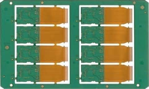
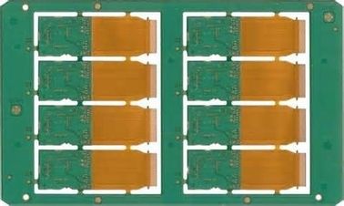
•  HDI Printed Circuit Board

Pacific PCB is a leading production company specialized in producing small quantity and diverse PCB prototypes. We manage fast time-to market to the standard for quality assurance.


• General Manufacturing Capability

Category Description Capability
File Formats Gerber files- preferred 274-X,274-D,DPF,ODB++
Drill file X & Y coordinates, with tool sizes included
Size Max. finished dimensions 580mm x 800mm – Single/ Double-sided
550mm x 800mm – Multilayer
Board Thickness Standard 1.6mm ±10%
Min. Single/ Double-sided:0.2mm ±0.1mm
4-layer:0.4mm ±0.1mm
6-layer:0.6mm ±0.1mm
8-Layer:1.0mm ±0.1mm
10-layer:1.0mm ±0.12mm
12-layer:1.2mm ±0.12mm
32-layer:4.0mm ±0.4mm and above
Max. 6.3mm ±10%
Bow and twist < 7/1000
Copper Outer Cu weight 1oz ~ 10oz
Weight Inner Cu wight 1/3oz ~ 6oz
Laminate Materials FR4(High TG,halogen-free),FR5,ISOLA(FR408,370HR),TEFLON,POLYIMIDE,ROGERS(RO4003,RO4350,RO4450),Aluminum plate (Single,Double-sided)
FR4 Thickness 1.6mm
High TG FR4 (170 deg C) 1.6mm
Board Cutting Max. number of layers 32
Min. thickness for inner layers (Cu thickness are excluded) 0.07mm
Drilling Min. size 0.1mm
Max. size 6.0mm 
Drill Deviation ±0.002” (0.050mm)
PTH hole tolerance ±0.003” (0.075mm)
NPTH hole tolerance ±0.002” (0.050mm)
Angle of Countersink 80°,90°,100°,120°
Plating Min. hole size 0.0008” 
Aspect ratio 20
Etching Trace width tolerance ±20%
Min. trace width / space (1oz finished Cu weight starting from 1/3oz) 0.003”/ 0.003”(0.08mm)
Min. trace width / space  (1oz finished Cu weight starting from 1/2oz) 0.004”/ 0.004”(0.1mm)
Min. trace width / space (2oz finished Cu weight) 0.005”/ 0.005”(0.127mm)
Min. trace width / space  (3oz finished Cu weight) 0.008”/ 0.008”(0.2mm)
Min. trace width / space (4oz finished Cu weight) 0.012”/ 0.012” (0.3mm)
Inner Layers Min. space from drilling to inner pattern 0.1mm
Min. space from annular ring to inner pattern 0.1mm
Layer-to-layer registration ±0.003”(0.08mm)
Solder Mask Color green,light green,matte green,white,extreme white,black,matte black,dark brown,yellow,red,blue,transparent
Min. solder mask clearance 0.003”
Thickness 0.0004”
Silkscreen Color White,black,yellow,red,blue,green
Min. trace width 0.005”
Min. size 0.028” / 0.028”
Electrical Test AOI  Y
Flying Probe Tester Y
Controlled Impedance Tolerance ±10%
Impedance tester Tektronix TDS8200
Routing End Mills Test ±0.15mm(0.006”)
CNC Tolerance ±0.15mm(0.006”)
V-Cut Depth ±0.1mm(0.004”)
V-cut angle deviation ±0.1mm(0.004”)
Semi-hole Y
Surface Finish HASL,HASL pb free,immersion gold,immersion silver,immersion tin,O.S.P (Entek),S/G plating,ENEPIG,G/F plating,carbon…
Blind and Buried Vias 3+N+3 Y
Resin,hole-filling ink,PTH Y
Others UL Cert. Y
ISO Cert. ISO9001/ISO14001/RoHS

Pacific PCB’s transparent factory allows our customers to witness the fascinating process of PCB production!


FR4,6 Layers Rigid flex PCB board Lead free HASL , 3 OZ Copper

Rincian kontak
PCB Board Online Marketplace

Kontak Person: Miss. aaa

Tel: 86 755 8546321

Faks: 86-10-66557788-2345

Mengirimkan permintaan Anda secara langsung kepada kami (0 / 3000)