pengantar
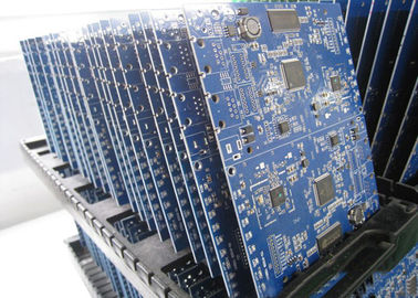
Kaku fleksibel papan sirkuit tercetak adalah papan menggunakan kombinasi teknologi papan fleksibel dan kaku dalam sebuah aplikasi. Kebanyakan papan fleksibel kaku terdiri dari beberapa lapisan sirkuit substrat yang fleksibel yang melekat pada satu atau lebih kaku papan eksternal dan / atau internal, tergantung pada desain aplikasi. Substrat fleksibel dirancang untuk berada dalam keadaan konstan fleksibel dan biasanya dibentuk menjadi kurva tertekuk selama manufaktur atau instalasi.
Desain fleksibel kaku lebih menantang daripada desain lingkungan papan kaku khas, seperti papan ini dirancang dalam ruang 3D, yang juga menawarkan efisiensi ruang yang lebih besar. Dengan mampu merancang dalam tiga dimensi yang kaku desainer fleksibel dapat memutar, melipat dan menggulung substrat papan fleksibel untuk mencapai bentuk yang diinginkan untuk paket aplikasi akhir ini.
Jenis bahan
FR-4, CEM-1, CEM-3, IMS, TG Tinggi, High Frequency, Halogen Gratis, dasar Aluminium, logam dasar inti
Pengobatan permukaan
HASL (LF), Flash emas, ENIG, OSP (lead free kompatibel), tinta karbon,
Peelable S / M, Immersion Ag / Tin, Gold jari plating, ENIG + Emas jari
Proses produksi
Apakah memproduksi prototipe atau produksi fleksibel kaku jumlah yang membutuhkan skala besar fabrikasi kaku fleksibel PCB dan perakitan PCB, teknologi ini terbukti baik dan dapat diandalkan. Bagian PCB fleksibel sangat baik dalam mengatasi ruang dan berat masalah dengan derajat tata ruang kebebasan.
Pertimbangan cermat solusi flex-kaku dan penilaian yang tepat dari pilihan yang tersedia pada tahap awal dalam tahap desain PCB fleksibel kaku akan kembali manfaat yang signifikan. Hal ini penting kaku fleksibel PCB FABRICATOR terlibat pada awal proses desain untuk memastikan desain dan bagian fab keduanya dalam koordinasi dan mempertimbangkan variasi produk akhir.
Tahap manufaktur fleksibel kaku juga lebih kompleks dan memakan dari fabrikasi papan kaku waktu. Semua komponen fleksibel perakitan fleksibel kaku memiliki sama sekali berbeda penanganan, etsa dan solder proses dari yang kaku papan FR4.
Aplikasi
LED, telekomunikasi, aplikasi komputer, pencahayaan, mesin permainan, kontrol industri, listrik, mobil dan high-end elektronik konsumen, ect.a
|
Detail produk:
|
Cahaya Tinggi: | Lead Free PCB,High Frequency PCB |
---|
1oz LED Display Rigid PCB Board FR4 4 Layer Blue Soldermask
PCB Name: | LED Display PCB Board | Layer count | 4 Layer |
Base Material: | FR4 | Board Thickness: | 1.6mm |
Copper Thickness: | 1oz | Min. Hole Size: | 0.4mm |
Min. Line Width/Spacing: | 0.15mm/0.15mm | Surface treatment: | Immersion Gold |
Solder mask color: | Blue | Silkscreen color: | White |
Original: | PCB Shenzhen House | Service: | PCB & PCBA |
Description:
China printing circuit board house specializes in PCB prototype and low volume PCB production manufacturing. Our printing circuit board manufacturing lines are located in China, which enable us to provide high quality, tight tolerance printed circuit boards at competitive prices.
From our printing circuit board, you are able to get instant contact with us to get online PCB quote only to tell us you requirement and send us PCB Gerber. Our team is waiting for you.
Applications:
Control Systems, LED Display, Digital Theater Systems, Vacuum Tube Electronics Displays, Linear Motors and Motion Products, Computer Diagnostic Tools, Lottery Pull-Tab and Scratch-off Ticket Machines, Point-of- Sale (POS) Electronic Security Systems, Automated ITVMs (Ticket Machines), Self-Service ATMs and Kiosks, Security Door Controls, Door Card Control, Electronic Lock, Aircraft Parts/Equipment, Switching Systems, Terminal Equipment, Publicly Accessible Equipment Vending Machines, Precision Positioning Systems, Robotics System, Water Purification System, Antenna, Guitar Electronics, Position Indicators, Controllers, Memory and Non-Memory Products, Networking, Wireless Communications ect.
Specification:
Layer count |
Single sided, 2L, 4L,6L,8L,10L-26 Layers |
Base material |
FR4, High Tg FR4, CEM-3, Aluminum Base, Copper core, High frequency, Polyimide (PI), Polyester(PET) ,Rogers RO4350,Polyimide,Teflon,Getek Copper Clad Thermal Substrates |
Board thickness |
0.2mm, 0.4mm, 0.8mm, 1.0mm. 1.2mm.1.6mm.2.0mm-2.4mm, 3.2mm,4.0mm |
Maximum Board Size |
580mmx700mm |
Copper thickness |
0.5oz, 1oz, 2oz ,3oz., 4oz,5oz,6oz |
Minimum Hole Size |
0.2mm |
Minimum Trace/Space |
4mil/4mil |
Surface finish |
HASL(Hot Air Solder Level), Pb Free HASL , Electroless Nickel and Immersion Gold (ENIG), Plating Gold, Gold Fingers (Gold Connector), Silver Immersion, Organic Surface Protectant (OSP), Electroless Nickel Electroless Palladium Immersion Gold (ENEPIG),Hard Gold |
Solder Mask |
Green, Red, Blue, Black, Matte Green, Orange |
Silk Screen |
White, Yellow, Black |
PCB Fabrication |
Scoring, Route, V-Score, Counter Sink, Bevel, Cutouts and Slots |
Quality Control |
IPC 6012 Class 2, Electrical Testing, Flying probe Testing, 100% Netlist Testing |
Special Technology |
Impendence Control, Differencial PCB printed circuit board, Peelabemask PCB , High Density PCB HDI, Carbon Ink Printing,Heavy copper PCB ,Metal Core circuit boards ,Copper Clad PCB printed wiring board, Blind & Buried Vias, Laser Drilled Vias, Burn-in Boards,Backplanes, Bonded heat sinks, Controlled depth drilling, Controlled Impedance, Filled/plugged vias, Heavy copper, HDI, Large format PCB, Landless vias, Printed Electronics, RF
|
Advantage:
1. We offer low-cost PCB prototypes. No minimum order limit.
2. Fast quotation, 24 hour prompt response.
3. Our PCB factory is ISO/TS approved and with high & advanced production capabilities.
4. We are full service provider. Our services include PCB manufacturing, PCB assembly, components sourcing, stencil, also PCB layout, from specification to final production turnkey service. It is your good choice for one stop PCB solutions.
5. We provide technical and professional support, satisfactory customer service.
Contact us with your detail PCB requirement Now!
Kontak Person: Miss. aaa
Tel: 86 755 8546321
Faks: 86-10-66557788-2345