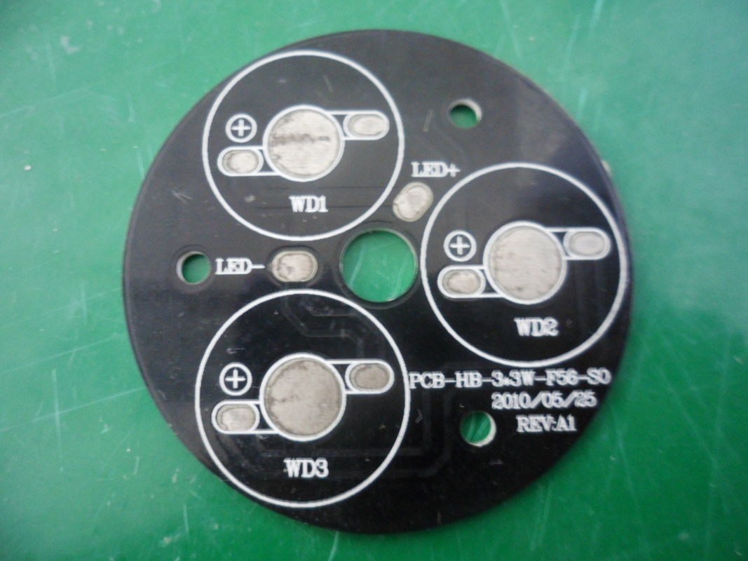
Cree High Power LED PCB / LED Light PCB Board Assembly 0.3mm - 3mm
Professional PCB Manufacturing
Base Material: Aluminum/FR4/CEM1/CEM3
Layer: 1 layer/2 layers
Board Thickness: 0.3-3mm
Min.Board Dimension: 4x4mm
Max.Board Dimension: 1500x600mm
Copper layer: 1oz/2oz/3oz
Solder Mask: White/Black/Blue/Red
Silkscreen: Black/White
Surface finish: LF HAL/HAL/OSP/Gold immersion/Silver plating
Outline Profile: CNC routing/V-Cut/Punching
All of the parameters can be customized!
Professional PCB Assembly:
Professional Surface-mounting and Through-hole soldering Technology.
Various sizes like 1206,0805,0603 components SMT technology.
ICT(In Circuit Test),FCT(Functional Circuit Test) technology.
PCB Assembly With UL,CE,FCC,Rohs Approval.
Nitrogen gas reflow soldering technology for SMT.
High Standard SMT&Solder Assembly Line.
High density interconnected board placement technology capacity.
Assemble pcb for you,plz click here
Our Quality Requirement:
We are now implementing international quality system includes: UL(E465880) ,TS16949 ,ISO14001, ISO9001
Quality target:
on-time delivery:≥98% ;
double layer board acceptability:≥97%
four-layer board acceptability:≥95%
six-layer board acceptability:≥92%
eight-layer board acceptability:≥88%
ten-layer board acceptability:≥85%
customer satisfaction :≥98%
complaint rate/rejected rate:≤ 1%
Our Environment Policy:
We committed to:
Comply with environmental regulations
Prevent any environmental accidents
Prevent pollution and reduce wastage
Minimize the consumption of resources
Education our employee in the awareness of the environmental protection
Set up environmental Management system and strengthen environment policy
RoHS compliance and Lead Free
Applications
It can be use 2835,5630,3014,5050,3525,CREE,Nichia,Osram LEDs
For all kinds of LED light
Lead Time
Samples: 3-4 days
Mass Production: 7-15 days(depend on the quantity)
Payment Terms
T/T,Western Union
Packing and Shipment
Vacuum package in carton

Factory Capability
|
Item
|
Manufacturing Capability
|
|
Surface Treatment
|
OSP
Immersion Gold Immersion Silver Immersion Tin Lead Free HAL Plating Silver
|
|
PCB Layer Type
|
Single side,Double side
|
|
Max. Working Panel Size
|
1500mm*600mm
|
|
Min. Working Panel Size
|
4mm*4mm
|
|
AL Substrate Thickness
|
0.3mm-4mm
|
|
Min. Conductor width
|
0.15mm
|
|
Min. Conductor spacing
|
0.15mm
|
|
Min. Drilling hole size
|
0.2mm
|
|
Plate Thickness Tolerance
|
±0.1mm
|
|
Finished Panel Tolerance
|
±0.1mm
|
|
V-CUT Alignment
|
±0.1mm
|
|
Hole Dia Tolerance
|
±0.05mm
|
|
Hole Position Tolerance
|
±0.076mm
|
|
Finished Copper Thickness
|
35um-105um(1oz-6oz)
|
|
Etching Under Cut
|
>/=2.0
|
|
PTH&Panel Plating Uniformity
|
>90%
|
|
Eing/Flash Gold Thickness
|
1-5u’’
|
|
Solder Mask Thickness
|
15um-35um
|
|
Min. Solder Mask Bridge
|
0.076mm(3mil)
|
|
Silk Screen
|
White/Black(depend on your requirements)
|
|
Thermal Conductivity
|
1.0~20W/MK
|
|
Withstand Voltage
|
AC 2000V,DC 1500~4000V
|
JHD PCB Company overview
The production line
JHD PCB in the professional lighting fair
Purchase Tips
a. If you want to purchase our PCB, you should provide a formal Gerber files or *.pcb file or something like that.
b. If you want to purchase by large quantity, please ask by SQM.
c. If you want to purchase the PCBA, you should provide the Gerber files, *.pcb file , BOM list etc.
d. If you want to reproduce some exsited PCB board for you, please first provide very clear pictures , then if you are satisfied with our estimate quotation, then send us the real thing, so we can clone it for you.
e. If none of the above can help you, please contact us directly by Skype, QQ or Email. We are very glad to answer the questions you ask, your satisfaction is our final destination.
JHD PCB would like to be your reliable partner in near future!

 Pesan Anda harus antara 20-3.000 karakter!