General Specifications Capability
Material Requirements:
| Size |
Max.Finshed Size |
20.9”x24.4”(530mm x 620mm ) |
| Board Thickness |
Standard |
0.004”to0.16 ” ±10% ( 0.1mmto4.0mm±10% ) |
| Min. |
Single/ Double-sided:0.008”±0.004”(0.2mm ±0.1mm) |
| 4-layer:0.01”±0.008”(0.4mm ±0.1mm) |
| 8-layer :0.01”±0.008”(0.4mm ±0.1mm) |
| Bow and twist |
< 7/1000 |
| Copper Weight |
Outer Cu weight |
0.5oz ~ 3.0oz |
| Inner Cu wight |
0.5oz ~ 3.0oz |
| Laminate Materials |
FR-4,FR-1,,FR-2,CEM-1,CEM-3 |
Process Requirements:
| Solder Mask |
Color |
green,light green,white,black,dark brown,yellow,red,blue |
| Min. solder mask clearance |
0.003”(0.07mm) |
| Thickness |
0.0005”-0.0007”(0.012mm-0.017mm) |
| Silkscreen |
Color |
White,black,yellow,red,blue,green |
| Min. Size |
0.006”(0.15mm) |
| Surface Finish |
HASL,HASL pb free,immersion gold,immersion silver,immersion tin,O.S.P (Entek),S/G plating,ENEPIG,G/F plating,carbon |
Quality Control:
| Electrical testing |
Flying Probe Tester |
Y |
| Controlled Impedance |
Tolerance |
±10% |
| Impedance tester |
Tektronix TDS8200 |
| Routing |
End Mills Test |
± 0.006”(0.15mm) |
| CNC Tolerance |
±0.004”(0.1mm) |
| V-Cut Depth V-cut |
FR-4(1/3+-0.1mm);FR-1,FR-2,CEM-1,CEM-3(1/2+-0.1mm) |
| V-cut angle V-CUT |
15°,18°,30° |
| V-CUT |
line,hole,V-shape |
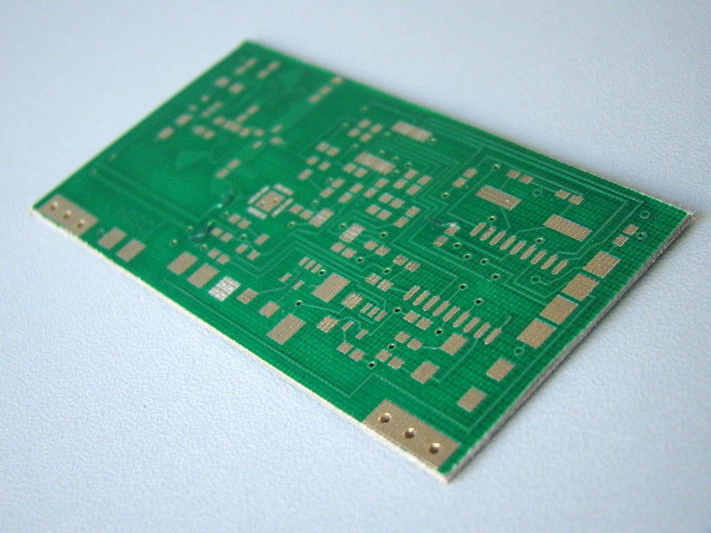
Manufacturing Capability for PCB Board
1). Material type: CEM-3,FR-4,FR-4-TG170/TG180,Halogen Free,Rogers,Arlon,Taconic,Isola,PTFE, Bergquist
2). Surface Treatment: HASL,HASL lead-free,HAL,Flash gold,immersion gold,OSP,Gold Finger
Palting,Selective thick gold plating, immersion silver,immersion tin, Carbon ink,peelable mask
3). Solder mask colour: Green/MATT Green/Blue/Yello/White/Black/Red
4). Board Size: 650mm*1000mm
5). Board Layer: 1L-26L
6). Board thickness: 0.2mm to 6.0mm
7). Finished Copper thickness: 0.5 OZ to 6 OZ
8). Min. drilled hole size: 3mil (0.075mm)
9). Min. Line width/Line spacing: 3mil/3mil
10). Copper thickness in hole: >20um
11). Board thickness tolerance: ±10%
12). Outline tolerance: Routing:±0.1mm,Punching:±0.1mm
13). Hole tolerance: PTH: ±0.076mm , NPTH: ±0.05mm
14). impedance control tolerance: ±10%
15). Warp and Twist: <0.75%
16). Tested by:Flying-Probe Tester, Fixture tester , Visual Inspection
17). Special requirements: Buried and blind vias, impedance control, thick Cu PCB,selectivity plating gold 30 microinch
18). Profiling: Punching, Routing, V-CUT, Beveling
19). Certificate: UL,ISO 9001,ISO14001,ROHS
20). We have a sound quality management system,Ensure the quality of all products
High precision manufacturing
Our Principle is simple, “Act by heart, Make the best.”
Our Strength is distinct, “Years of experiences in PCB and PCBA field”
Our Goal is achievable, “ To be the most reliable supplier of PCB and PCBA.”
Our Orientation is clear, “Focus on prototypes and low to medium volume business ”

 Pesan Anda harus antara 20-3.000 karakter!