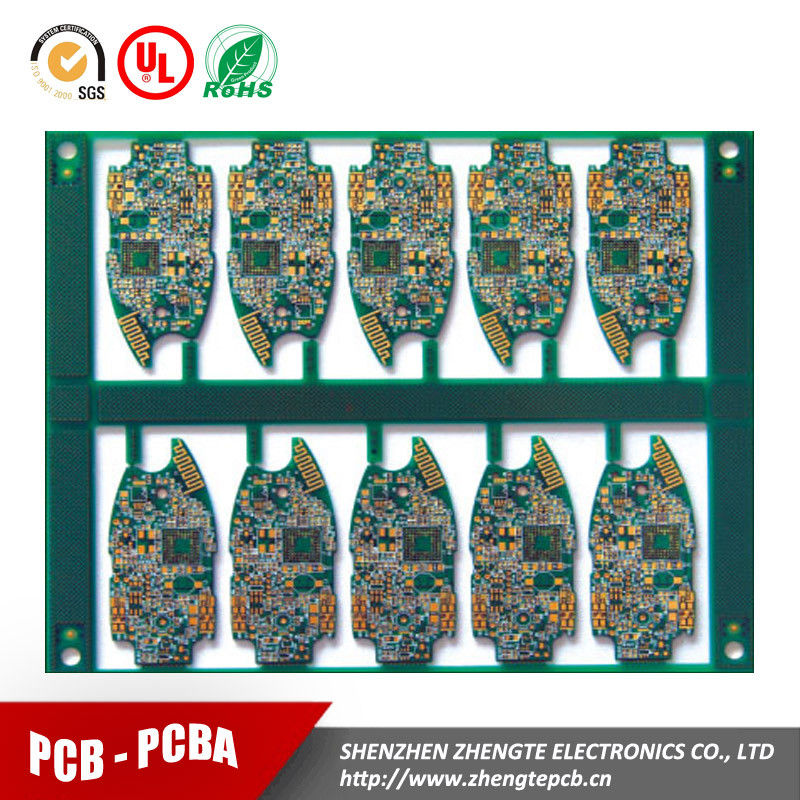
Zhengte Electronics PCB&PCBA Contract Manufacturing Services Including Belows:

Single-side PCB Double-side PCB and Multilayer PCB PCBA
1.Fast PCB Fabrication for Samples and Mass Production
2.Electronic Components Sourcing Servics
3.PCBA Assembly Services:SMT,DIP,BGA...
4.Function Test
5.Stencil and Enclosure Assembly
6.Standard Packing and On time Delivery
Main Products Application
1.Household Appliances
2.Medical Products
3.Automotive Products
4.Industrial Products
5.Communication Products(AVL/GPS/GSM Devices)
6.Consumer Electronics
PCB Fabrication Capabilities
| Number of Layer | 1,2,4 or 6,upto 18 layer |
| Order Quantity | 1 to 50,000 |
| Board Shape | Retangular,round,slots,cutouts,complex,irregular |
| Board Type | Rigid, Flexible, Rigid-flexible |
| Board Material | FR-4 glass epoxy, FR-4 high Tg, Rohs compliant,Aluminum,Rogers,etc. |
| Board Cutting | Shear,V-score,Tab-routed |
| Board Thickness | 0.2-4.0mm, Flex 0.01-0.25mm |
| Copper Weight | 1.0, 1.5, 2.0 oz |
| Solder Mask | Double-sided green LPI,Also support Red,White,Yellow,Blue,Black |
| Silk Screen | Double-sided or single-sided in white,yellow,black,or negative |
| Silk Screen Min Line Width | 0.006'' or 0.15mm |
| Max Board Dimensions | 20 inch*20inch or 500mm*500mm |
| Min Trace/Gap | 0.10mm, or 4mils |
| Min Drill Hole Diameter | 0.01'',0.25mm, or 10mils |
| Surface Finish | HASL,Nickle,Immersion Gold,Immersion Tin,Immersion Silver,OSP,etc. |
| Board Thickness Tolerance | ±10% |
| Copper Weight Tolerance | ± 0.25 oz |
| Minimal Slot Width | 0.12'', 3.0mm, or 120mils |
| V-Score Depth | 20-25% of board thickness |
| Design File Formate | Gerber RS-274,274D,Eagle and AutoCAD's DXF,DWG,PCB file |
PCB Assembly Capabilities
Quantity | Prototype&Low Volume PCB Assembly,from 1 Board to 250,is specialty,or up to 1000 |
| Type of Assembly | SMT,Thru-hole |
| Solder Type | Water Soluble Solder Paste,Leaded and Lead-Free |
| Components | Passive Down to 0201 size BGA and VFBGA Leadless Chip Carriers/CSP Double-sided SMT Assembly Fine Pitch to 0.8mils BGA Repair and Reball Part Removal and Replacement |
| Bare Board Size | Smallest:0.25*0.25 inches Largest:20*20 inches |
| File Formate | Bill of Materials Gerber files Pick-N-Place file |
| Types of Service | Turn-key,partial turn-key or consignment |
| Component packaging | Cut Tape,Tube,Reels,Loose Parts |
Turn Time | Same day service to 15 days service |
Testing | Flying Probe Test,X-ray Inspection AOI Test |
| PCB assembly process | Drilling-----Exposure-----Plating-----Etaching & Stripping-----Punching-----Electrical Testing-----SMT-----Wave Soldering-----Assembling-----ICT-----Function Testing-----Temperature & Humidity Testing |
PCB Lead Time
| Layer/Days | Sample(Normal) | Sample(Fast) | Mass Production |
| Single/Double | 3-5days | 24-72hours | 7-10days |
| Four Layer | 5-7days | 5days | 7-12days |
| Six Layer | 10-12days | 8days | 13-15days |
| Eight Layer | 15-20days | 7-10days | 16-20days |
Detailed Terms for PCB Assembly
1.Technical requirement for pcb assembly: What we can do?
1) Professional Surface-mounting and Through-hole soldering Technology
2)Various sizes like1206,0805,0603,0402,0201 components SMTTech
3) ICT(In Circuit Test),FCT(Functional Circuit Test) technology
4) PCB Assembly With UL,CE,FCC,Rohs Approval
5) Nitrogen gas reflow soldering technology for SMT
6) High Standard SMT&Solder Assembly Line
7) High density interconnected board placement technology capacity
2.Production Details:
1) Material Management
Supplier → Components Purchase → IQC → Protection Control →Material Supply → Firmware
2) Program Management
PCB Files → DCC → Program Organizing → Optimization → Checking
3) SMT Management
PCB Loader → Screen Printer → Checking → SMD Placement →Checking → Air Reflow → Vision Inspection → AOI → Keeping
4) PCBA Management
THT→Soldering Wave (Manual Welding) → Vision Inspection → ICT →
Flash → FCT → Checking → Package → Shipment
3.Our Advantage:
1.Related Certificate --- UL ,ISO9001:2000 , TS16949, Rosh.
2.100% electrical test, AOI testing, four times 100% QC inspection beofre shipping.
3.High reliable, Germany equipment ,competitive price andSpeedy delivery.
4.Fast Prototype Service.
5.One stop electronic assembly service(provide prototype, plastic injection molding, part painting,
components purchasing, SMT COB,DIP,PCBA service as one unit).
4.Package:
RFQs
1.How can I get quotation in time?
Please send us the PCB File and Components list via mail or Online tool(Aliwangwang or Skype,WhatsApp)
The file will be checked and the initial quotation will be offered withing 2 working days as usual
(Gerber,Eagle,PCB,CAD file are acceptable).
2.How to Place order with Zhengte Electronics?
Step1: Send us the PO with request (Final project files confirmed) and we will confirm with PI.
Step2: The order will be entered into our order system in same day.
Step3: Deposit or full payment complete,then order confirmed by our financial department.
Step4: The order will be proceed accordingly by our purchasing system.
Step5: Sample or photos offered for approval.
Step6: Balance payment complete,shippment arranged and tracking will be offered via email.
3.What's the normal sequency of order?
Step1: * PCB board file with parts list details provided by customers.
Step2: * PCB board file checked by PCB engineer.
Step3: * PCB board components sourced by Zhengte Electronics.
Step4: * Components checked by Zhengte Electronics warehouse stuffs.
Step4: * PCB board with components assembled.
Step5: * Electronic testing circuit board or PCBA.
Step6: * Anti-static package,Fast delivery.
4.How can make sure no mistake for mass production?
The production files will be checked by our engineering teams.Samples will be
offered for approval before mass production.
5.What files in need for the PCB Assembly services?
Besides the PCB files and Components list,we also need PNP(Pick and Place)
and Components Position files for production.
6.How can I track the shipment?
When order complete,an email will be sent out to confirm the value and shipment methods.
Then the shipment tracking number will be shared with email as always.
7.How can I share the feedback?
Please send the comments with the order number within 30days to our feedback service department.
Our service department will proceed in working days as usual.
8.What service Zhengte Electronics can offer?
One stop service for PCB design,PCB layout,PCB manufacture,Components purchasing,PCB assembly,Testing,Packing and PCB delivery.
Quality Control
CONTACT USSHENZHEN ZHENGTE ELECTRONICS CO., LTD.
Tel:86-0755-25585656 EXT.801 Fax:86-0755-25563466
Website: www.zhengtepcb.cnWhatsapp/Mobile: 0086-15814076116Skype:pcba.solutions

 Pesan Anda harus antara 20-3.000 karakter!